
7 Common Mistakes When Using Conductive Filaments (and How to Avoid Them)
Conductive filaments open exciting possibilities for printing electronics directly into 3D printed parts—but they also come with unique design and processing challenges. In this article, we highlight seven common mistakes engineers and makers make when working with conductive filaments and share practical tips based on our experience using Electrifi conductive filament for antennas, embedded circuits, and functional prototypes.
ELECTRIFI ENGINEERING SERIES
3/5/20263 min read
Conductive filaments open the door to a new design space where electrical functionality can be integrated directly into 3D printed structures. With materials like Electrifi conductive filament, engineers and makers can print antennas, heaters, sensors, and embedded circuits using standard FFF printers.
However, conductive filaments behave very differently from conventional plastics—and even differently from traditional metals used in electronics.
Over the years, we have observed several common pitfalls when users first begin working with conductive materials. Understanding these early can significantly improve your results and help you get the most out of Electrifi.
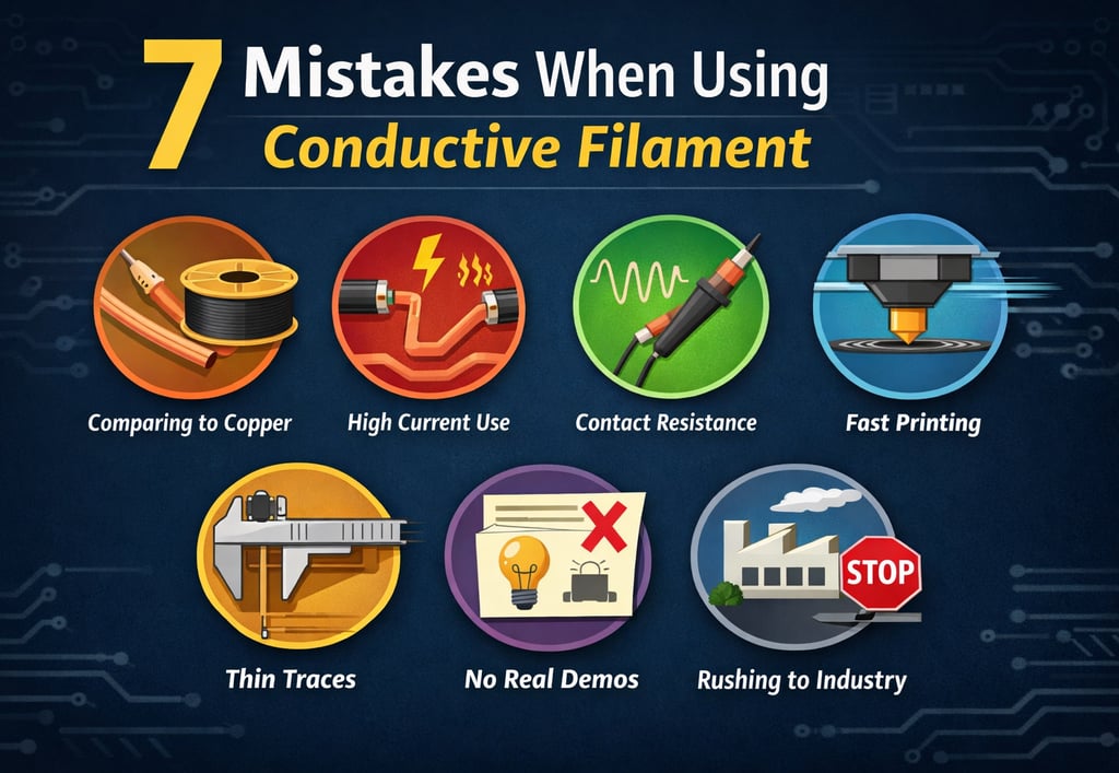
1. Expecting Conductive Filament to Replace Copper
One of the most common misconceptions is that conductive filament should behave like solid copper wire or PCB traces.
Copper has an electrical conductivity of approximately:
5.8 × 10⁷ S/m
Even the most conductive printable composites operate at lower values. Electrifi typically reaches conductivity levels up to ~10⁵ S/m, which is orders of magnitude higher than carbon-based conductive filaments but still lower than bulk metals.
Rather than replacing copper, Electrifi enables design possibilities that traditional wiring cannot easily achieve, such as:
embedded conductive pathways
complex RF structures
conformal antennas
structural electronics.
When the focus shifts from “replacing copper” to integrating electronics into printed structures, the real advantages become clear.
2. Using Conductive Filament for High-Current Applications
Conductive filaments are not designed for high current power distribution.
Long traces carrying significant current will experience:
voltage drop
resistive heating
efficiency losses.
Electrifi works best in applications where geometry and integration matter more than current capacity, such as:
RF antennas
sensors
inductive coils
EMI shielding structures
printed heaters.
For these use cases, Electrifi provides a unique balance of conductivity and manufacturability.
3. Ignoring Contact Resistance
In many printed electrical structures, the largest resistance does not come from the printed trace itself, but from the electrical interface between the trace and measurement probes or connectors.
Poor contact can significantly distort resistance measurements.
To obtain reliable results, users often:
apply silver paste or conductive coating to the probe points
use mechanical compression contacts
design larger contact pads.
Reducing interface resistance helps reveal the true conductivity of the printed structure.
4. Printing Too Fast
Conductive filaments typically contain high filler loading, which changes their flow behavior compared with standard PLA or PETG.
Printing too quickly can lead to:
unstable extrusion
poor layer bonding
inconsistent conductivity.
Electrifi prints best when treated with care rather than speed. Typical recommendations include:
slower print speeds (10–30 mm/s)
larger nozzle diameters (≥0.4 mm, preferably 0.6 mm)
minimal retraction.
Slower printing often leads to better electrical and mechanical performance.
5. Designing Traces That Are Too Thin
Many new users design conductive traces similar to PCB traces, which are often fractions of a millimeter wide.
With conductive filament, trace geometry plays a major role in electrical performance.
To reduce resistance:
use wider traces
increase trace thickness
minimize trace length when possible.
For most applications, 100% infill is recommended for conductive features.
6. Skipping Real Functional Demonstrations
Conductive filaments are sometimes tested only by measuring resistance across a small printed sample. While this provides useful data, it does not fully demonstrate the potential of the material.
The most effective way to understand Electrifi is through functional components, such as:
antennas
inductive coils
embedded LED circuits
EMI shielding enclosures
conductive gaskets.
These demonstrations highlight the true value of Electrifi: combining electrical functionality with additive manufacturing.
7. Targeting Large Industrial Applications Too Early
Many advanced materials aim immediately for large industries such as automotive or aerospace. However, these sectors often require extensive testing, certification, and supply chain validation.
Instead, conductive filaments often gain traction first in:
research laboratories
engineering prototyping
university projects
advanced maker communities.
These early adopters explore new ideas and publish results that gradually expand the technology’s reach.
Electrifi has already been used in several research projects exploring RF devices, antennas, and printed electronics, helping demonstrate the possibilities of conductive additive manufacturing.
Final Thoughts
Electrifi represents a new category of material—a conductive structural polymer designed for additive manufacturing. Its value does not come solely from electrical conductivity, but from the ability to integrate electrical functionality directly into printed parts.
When used with the right design approach and printing strategy, Electrifi enables applications that are difficult—or sometimes impossible—to achieve with traditional electronics manufacturing methods.
As more engineers and researchers explore this design space, we expect to see many new innovations emerging from 3D printed conductive structures.