
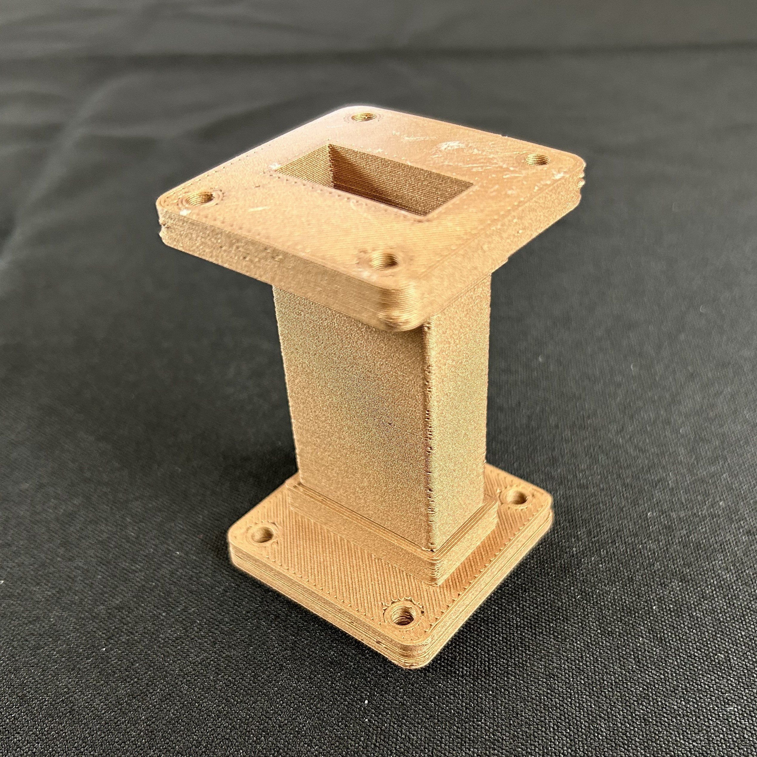
Electrifi™ WR112 Straight Waveguide
Operating From 7.05 GHz to 10 GHz
$251.00
Overview
The Electrifi™ WR-112 Straight Waveguide is a fully 3D printed microwave transmission structure designed for operation across the 7.05–10 GHz frequency range. Fabricated using Electrifi™ conductive filament, this component demonstrates the feasibility of conductive additive manufacturing for guided-wave microwave applications.
This straight section is compatible with WR-112 interface dimensions and is intended for laboratory validation, signal transmission studies, and additive manufacturing benchmarking.
This product is offered as an engineering sample under the Electrifi™ Functional Prototype Validation Program.
Key Features
Designed for 7.05–10 GHz operation
WR-112 standard internal geometry
Fully dense (100% infill) conductive structure
Lightweight alternative to machined aluminum waveguides
Rapid fabrication via FFF additive manufacturing
Suitable for S-parameter characterization and insertion loss testing
Physical & Fabrication Specifications
Parameter | Specification |
|---|---|
Dimensions | 47.6 mm × 47.6 mm × 76.2 mm |
Weight | 85 g |
Material | |
Manufacturing Process | FFF (Fused Filament Fabrication) |
Nozzle Diameter | 0.6 mm |
Layer Height | 0.3 mm |
Infill | 100% |
The structure is printed fully solid to maximize electrical continuity and mechanical integrity.
Applications
Microwave transmission testing
S21 insertion loss measurement
Return loss (S11) benchmarking
Lightweight RF system prototyping
Educational microwave laboratory demonstrations
Engineering Sample Notice
This antenna is supplied as an engineering validation unit. Participants are encouraged to perform laboratory-grade measurements including:
S11 (return loss)
S21 (insertion loss)
VSWR
Frequency response characterization
Submitted measurement data may qualify for credit under the Electrifi™ Functional Prototype Validation Program.
Why Electrifi™ for RF Components?
Electrifi™ conductive composite enables:
Significantly higher conductivity than conventional conductive polymers
Direct fabrication on standard FFF platforms
Reduced lead time compared to CNC-machined metal waveguides
Rapid geometry modification for experimental studies
This waveguide serves as a reference geometry for evaluating conductor losses and surface roughness effects in additively manufactured RF components.
Electrifi™ functional prototypes are sealed with desiccant in moisture-barrier packaging and labeled with full material specifications.
Electrifi™ functional prototypes typically have a lead time of 5–6 business days. Once printing is complete, the parts are promptly processed and shipped via reliable carriers.
Domestic (U.S.) Orders: Typically delivered within 2–3 business days after shipment.
International Orders: Typically delivered within 3–6 business days, depending on destination and customs processing.
Tracking information is provided once your order has shipped.
We accept returns of unopened packages, no questions asked. Customers are responsible for return shipping costs unless the product is defective.